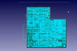
The proliferation of packaging designs that combine multiple chips into a single package is creating new challenges for package, printed circuit board (PCB) and integrated circuits (IC) designers. The common practice of designing the package, PCB and IC in standalone environments requires time-consuming manual processes that are error-prone and limit the potential for design reuse. What is needed are 3D co-design tools that integrate planning and final design implementation at the system level for PCBs, ICs, packages and mechanical enclosures.